Electromagnetics Research Lab
Principal Investigator: Adam Mock
About
The electromagnetics research lab (ERL) supports experimental work in visible to near infrared photonics, actively and passively mode locked fiber lasers, and experiments microstructured optical fibers.
It is located in room ET 121 of the Engineering and Technology building.
Equipment
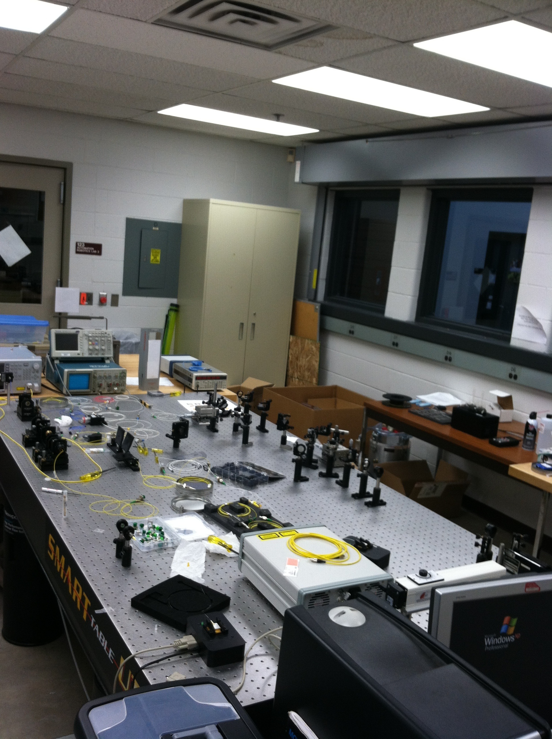
4 ft by 8 ft Newport vibration isolated optical table
Anritsu optical spectrum analyzer (600nm - 1750nm)
Two three-dimensional translation stages with sub-micron resolution (Newport)
Superluminescent diode at 1550nm
Semiconductor optical amplifier at 1550nm
Laser diodes at 1480nm and 1550nm
Free space to fiber coupling
Erbium doped fiber amplifier
High speed infrared detector
Frequency resolved optical gating (FROG) short pulse characterizaton system
Various fiber optics and optomechanical components (isolators, mirrors, lens, circulators, etc.)
Projects
(1.) Graphene mode-locked fiber lasers - The goal of this project is to generate sub-picosecond optical pulses using a fiber ring laser with a graphene
saturable absorber. The fiber ring laser is driven by an erbium doped fiber amplifier (EDFA). Graphene is a nanomateral that has received
considerable attention recently. Its experimental discovery in 2004 was awarded the 2010 Nobel prize in physics. It has a number of interesting
properties including exceedingly high mechanical strength and electrical conductivity. It also exhibits nonlinear absorption similar to that of single wall
carbon nanotubes. Applications of the ultrashort pulse fiber ring laser range from medicine to telecommunication. A specific application
considered in this project is micrometer laser micromachining of glass fiber. Achieving large pulse energy will be important for success in
this project.
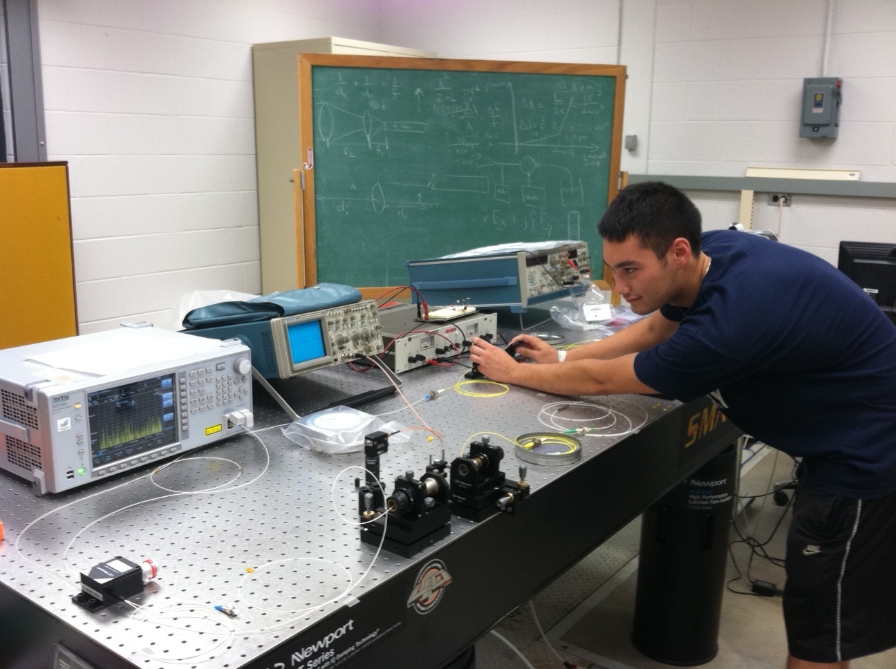
The image on the left shows CMU undergraduate student Waylin Wing working on the mode-locked fiber laser setup in the ERL.
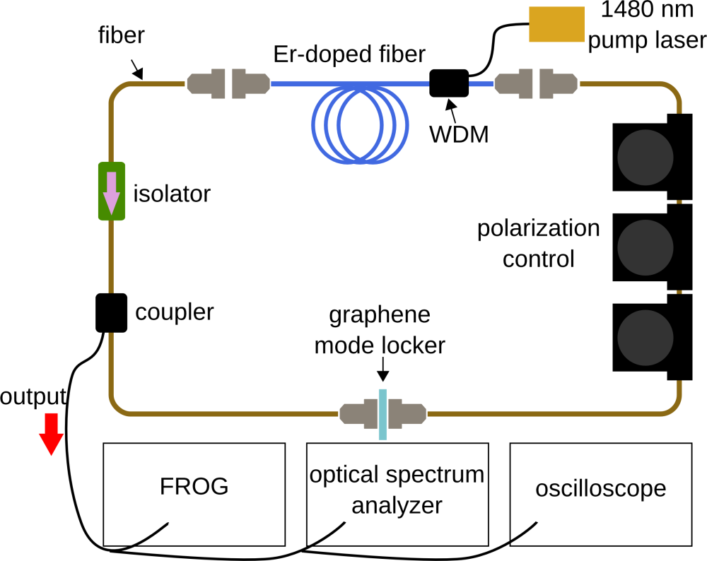
The image in the center displays a schematic drawing of the fiber ring laser setup. The image on the right
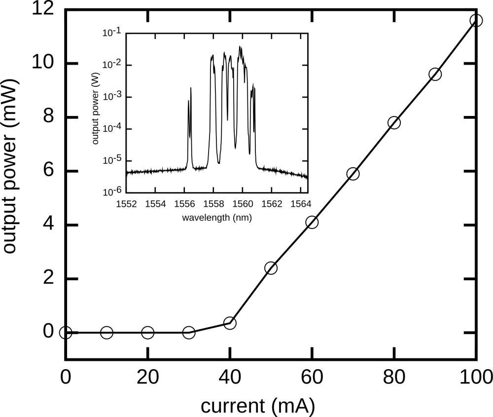
depicts the continuous wave output power of the fiber ring laser versus EDFA pump current. The inset is a multimode lasing
spectrum. All data taken in the ERL.
(2.) Infiltrated photonic crystal fiber devices - The goal of this project is to infiltrate the internal
air voids in photonic crystal fiber with optically influencing materials. These include colloidal quantum dot
solutions for optical amplification, gold or silver metal for surface plasmon devices or graphene for saturable absorption.
Infiltrating hollow-core microstructured optical fiber will lead to an enhanced and nearly ideal light-matter interaction promoting
larger gain coefficients in the case of quantum dot infiltration, improved surface plasmon coupling in the csae of metal infiltration,
and lower power for reaching intensity threshold in the case of graphene infiltration.
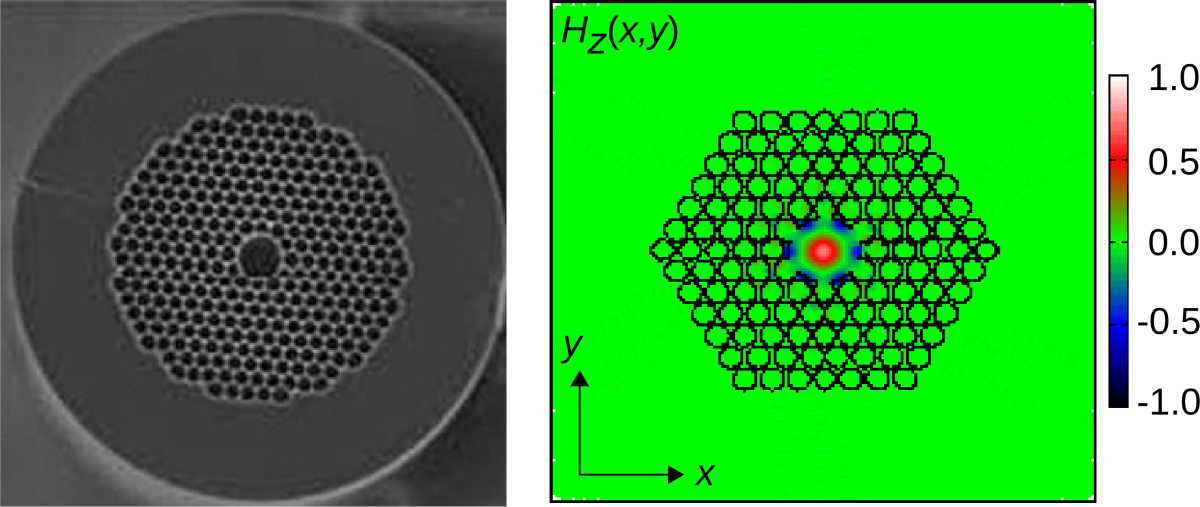
The image on the left below is a scanning electron micrograph of a hollow core microstructured optical fiber (courtesy of the manufacturer, Thorlabs).
The image on the right below is a compact FDTD similation performed in the ERL showing the magnetic field confinement at the center of the fiber core.
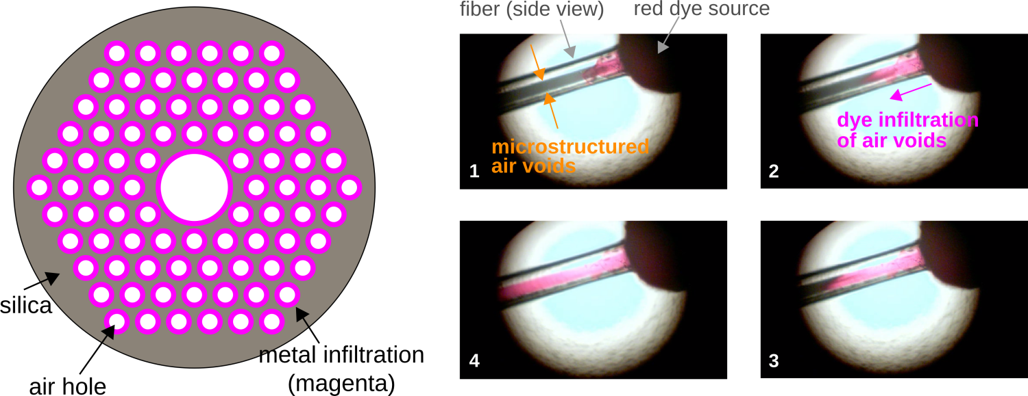
The image on the left is a schematic diagram of a hollow core microstructured optical fiber whose interior air voids have been coated with
metal. On the right, a progression of optical microscope images taken in the ERL depicts infiltration of a fiber with red dye.
(3.) Theoretical and computational design and analysis of micro-photonic and nano-photonic devices - The ERL utilizes
finite-difference time-domain methods for the electromagnetic analysis of photonic devices. The goal of this analysis is
the exploration of novel optical phenomena associated with geometrical features at or smaller than the wavelength of light.
The ERL utilizes high performance work stations at CMU as well as distributed computing at the
Michigan State University High Performance Computing Center .
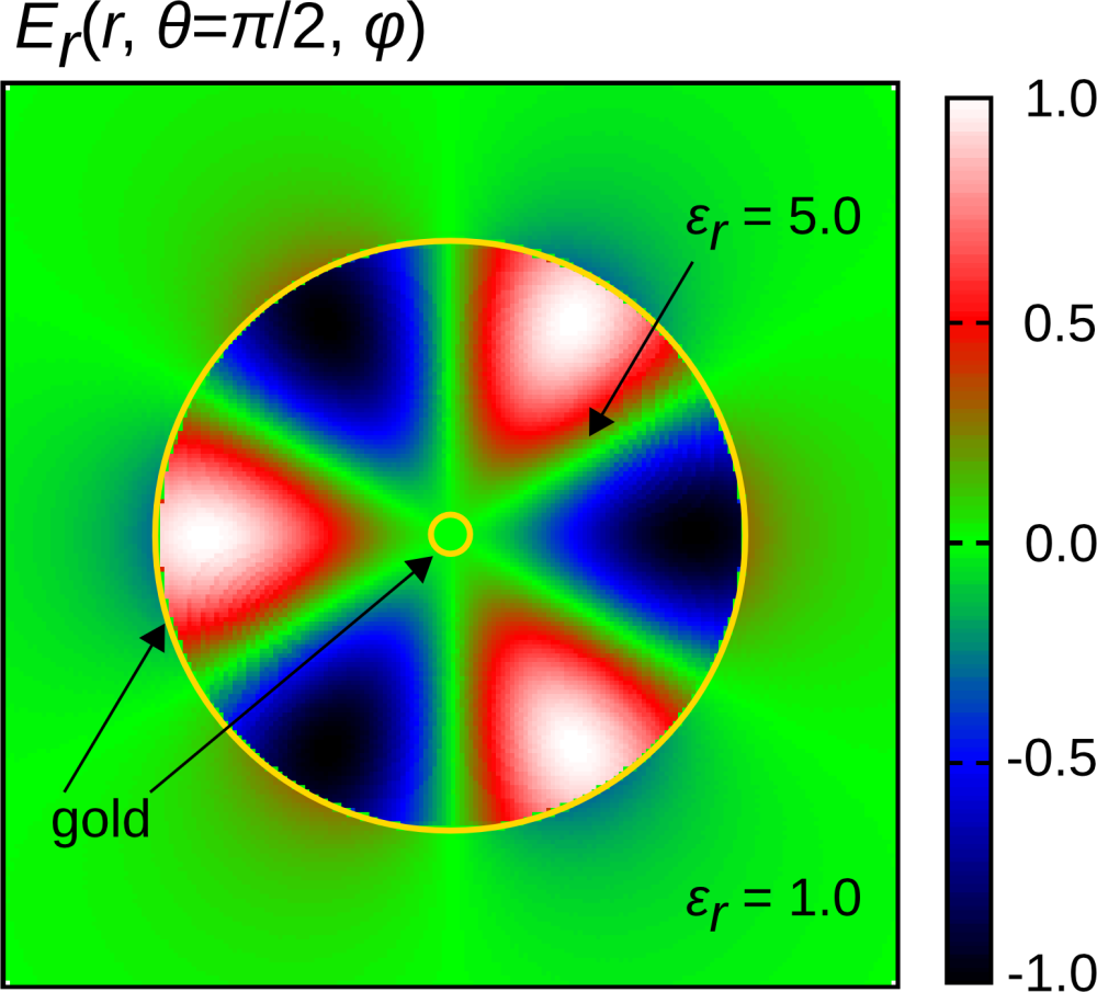
The image on the left below shows the radial component of the electric field inside of a double layer nanoplasmonic spherical resonator. The
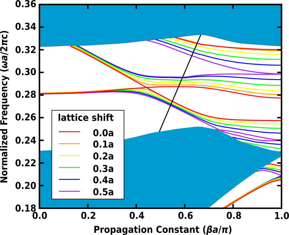
field was calculated using the compact FDTD method for structures with spherical invariance. The middle image below shows the photonic
crystal waveguide dispersion diagram of a two-dimensional photonic crystal single line defect waveguide with varying degrees of cladding shifts.
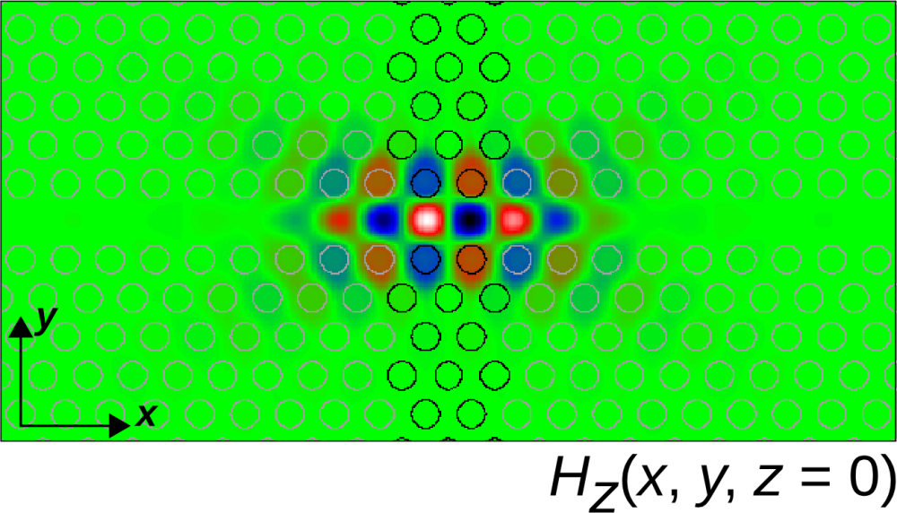
The image on the right is the magnetic field of a bound state mode of a photonic crystal double heterostructure cavity.